Whitepaper
AI Driven AOI-based Wafer Defect Classification System
Executive Summary
Automated Optical Inspection (AOI) systems have become indispensable in semiconductor wafer manufacturing, enabling high-speed, high-resolution detection and classification of wafer defects. The integration of advanced imaging technologies with artificial intelligence (AI) and deep learning (DL) techniques has significantly enhanced AOI capabilities, improving defect detection accuracy, classification precision, and throughput. This whitepaper explores the architecture, methodologies, and benefits of AOI-based wafer defect classification systems, emphasizing AI-driven approaches for optimized semiconductor yield and process control.
This AI-driven solution supports Mindteck’s objective of delivering high-performance inspection systems tailored for the semiconductor manufacturing industry.
Problem Statement
Wafer Defects and Their Impact
In semiconductor manufacturing, each wafer undergoes numerous complex processing steps, from deposition and lithography to etching and ion implantation. At every stage, there is a potential for defects to arise. These defects can manifest in various forms:
Pattern defects: Missing, extra, or malformed circuit patterns.
Particle defects: Contaminants (dust, debris) on the wafer surface.
Scratch defects: Physical damage to the wafer.
Bridge defects: Unintended connections between conductive lines.
Open defects: Breaks in conductive lines.
Residue defects: Unwanted material remaining after processing.
Structural defects: Crystalline imperfections or delaminations.
The consequences of undetected or misclassified wafer defects are severe:
Significant Yield Loss: Defective dies translate directly to reduced functional chips per wafer, drastically increasing per-chip cost.
Increased Rework and Scrap: Imperfect wafers may require costly rework or, more often, are scrapped entirely, wasting valuable materials and processing time.
Delayed Time-to-Market: Rework and retesting cycles extend production timelines, impacting a company's ability to capitalize on market opportunities.
Reliability Issues: Subtle defects that pass initial inspection can lead to premature device failure in the field, damaging brand reputation and incurring warranty costs.
Inefficient Process Control: Without accurate and timely defect classification, identifying the root cause of defects (e.g., equipment malfunction, process deviation, material impurity) becomes challenging, hindering effective process improvement.
Traditional manual visual inspection is slow, subjective, prone to human error, and incapable of detecting microscopic defects across an entire wafer. Older automated systems often struggle with the diversity and complexity of defect types, leading to high false-positive rates and limited classification accuracy.
Introduction to AOI in Semiconductor Wafer Inspection
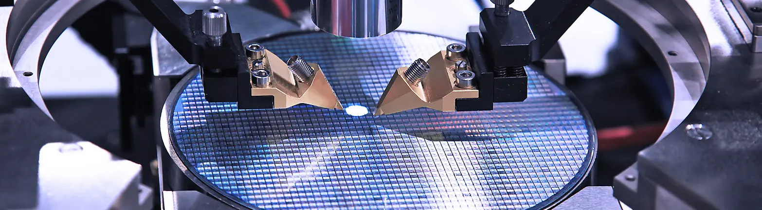
Automated Optical Inspection (AOI) is a non-contact, high-speed visual inspection technology used extensively in semiconductor manufacturing to identify surface and pattern defects on wafers. AOI systems capture high-resolution images under various lighting conditions and analyze these images to detect anomalies that could impact yield and device performance.
AOI serves as the first line of defence in quality control, inspecting wafers after critical process steps such as patterning, etching, and deposition. Unlike manual inspection, AOI operates at nanometer-scale precision, essential for modern semiconductor nodes with shrinking geometries and complex 3D structures.
AOI System Architecture and Workflow
Image Acquisition
AOI systems employ high-resolution cameras (up to 25 megapixels) mounted on precision stages to scan the wafer surface. Multispectral lighting (visible, UV, IR, polarized) is used to highlight different defect types, including particles, scratches, and topographical variations. Techniques like dark-field imaging enhance edge defect detection.
Preprocessing and Alignment
Captured images undergo preprocessing to normalize brightness, reduce noise, and geometrically align with reference patterns or "golden units." This step ensures consistent comparison and accurate defect localization by correcting for wafer shifts, rotations, or warping.
Defect Detection
Defect detection combines rule-based algorithms and statistical models:
Pattern matching to identify deviations from expected shapes
Edge detection for line breaks or mask misalignments
Anomaly detection using statistical deviations to find unknown defects
Morphological analysis for size, shape, and texture extraction
Defect Classification
Defect detection combines rule-based algorithms and statistical models:
Pattern matching to identify deviations from expected shapes
Edge detection for line breaks or mask misalignments
Anomaly detection using statistical deviations to find unknown defects
Morphological analysis for size, shape, and texture extraction
AI and Deep Learning in AOI-Based Defect Classification
AI-Driven Defect Analysis
Modern AOI systems integrate AI to enhance detection and classification accuracy. AI models can differentiate between cosmetic and critical defects, reducing false positives and improving decision-making. Techniques include:
Object detection for precise defect localization
Segmentation to isolate defects from background
Anomaly detection using unsupervised learning to identify novel defect types
Deep Neural Networks (DNN) for Wafer Defect Classification
Advanced deep learning models, such as ResNet, VGG, Inception, MobileNet or GoogLeNet architectures, have demonstrated state-of-the-art performance in classifying both single and mixed wafer defect patterns. These models achieve classification accuracies up to 99.9% by employing data augmentation techniques to address className imbalance and noise robustness.
Hybrid AI approaches combining Convolutional Neural Networks (CNN) and K-Nearest Neighbors (KNN) have shown breakthroughs in classification performance, reducing defect escape rates and improving inline AOI tool reliability.
Key Features of AI Driven AOI-Based Wafer Defect Classification Systems
High-Resolution Imaging:Sub-micron resolution imaging enables detection of the smallest defects.
Multispectral Lighting:Enhances visibility of diverse defect types, including subsurface anomalies.
Automated Focus and Precision Stages:Ensure consistent image quality across wafers.
Modular and Scalable Design:Facilitates customization and upgradeability.
AI-Powered Classification:Reduces manual intervention, improves accuracy, and accelerates throughput.
Traceability and Documentation:Generates detailed defect maps with timestamps and severity scores for process control and auditability.
Automated Material Handling:Integration with robotic arms for seamless wafer transfer during inspection.
Benefits of AI Driven AOI-Based Wafer Defect Classification
Yield Improvement: Early detection and accurate classification prevent defective wafers from progressing, reducing scrap rates.
Increased Throughput: Automated analysis reduces Manual Inspection effort by 75% – 90% without compromising quality.
Process Control Enablement: Defect data feeds into Statistical Process Control (SPC) and Yield Management Systems (YMS) to identify trends and root causes.
Reduced False Positives: AI classification minimizes unnecessary rework and inspection cycles.
Adaptability: Continuous learning AI models adapt to new defect patterns and process changes, maintaining inspection relevance in evolving manufacturing environments.
Cost Efficiency: Reduces manpower needs for visual inspection while improving overall inspection accuracy.
Applications and Use Cases
Front-End Wafer Inspection:Detecting pattern defects post-lithography and etching.
Back-End Packaging Inspection:Ensuring integrity during wafer-level packaging and singulated package inspection.
Post-Saw Inspection:Identifying sawing-induced surface defects.
3D Structure Inspection:Detecting topographical defects such as dishing and erosion using 3D AOI techniques.
Technology Stack
This section outlines the key technologies used in building the wafer defect classification system. It includes tools for image processing, machine learning, model deployment, integration, and visualization. The stack ensures performance, scalability, and seamless factory integration.
Component | Technologies Used |
|---|---|
Image Processing | OpenCV, scikit-image |
Learning Frameworks | PyTorch, TensorFlow, Keras |
Model Deployment | ONNX, TorchServe, TensorRT, MLflow, GoogleNet |
Deployment Platform | NVIDIA GPU, Triton Inference Server |
Integration | REST APIs, Kafka, MES/SCM systems |
Visualization | Streamlit, Plotly Dash, Grafana |
Deployment Strategy
The deployment approach ensures real-time performance and flexibility across different environments. It supports edge deployment for low-latency inference and cloud integration for scalable model management. Automation through CI/CD (MLOps) enables continuous improvements without hindering production.
Edge Deployment: Real-time classification on in-fab GPU devices.
Cloud/Hybrid: Model management and retraining pipeline hosted on cloud.
CI/CD: Automated retraining, testing, and deployment workflows.
API Integration: Connects with factory automation, MES, SPC, and FDC systems.
Challenges and Mitigation
Deploying a machine learning–based AOI system presents both technical and operational challenges. This section addresses common obstacles such as className imbalance, noise, and integration complexity. Proven mitigation strategies are listed to ensure system reliability and adaptability.
Challenge | Mitigation Strategy |
|---|---|
Class imbalance | Data augmentation, synthetic oversampling |
Image noise | Noise filtering and robust preprocessing |
Model drift | Scheduled retraining using feedback loops |
System integration | API-first architecture and modular design |
Conclusion
Mindteck offers this AI-driven AOI-based wafer defect classification system as a high-value solution in its semiconductor service portfolio. The system can be customized for client-specific inspection criteria, integrated into factory automation pipelines, and scaled across multiple fabs.
Glossary
AOI: Automated Optical Inspection
AI: Artificial Intelligence
CNN: Convolutional Neural Network
KNN: K-nearest Neighbors
SPC: Statistical Process Control
YMS: Yield Management System
3D AOI: Three-Dimensional Automated Optical Inspection
Published Date: July 14, 2025
Authors: Amitesh Dutta & Tanmoy Mondal
Co-Author: Saibal Dey
Get the insights you need
Access expert knowledge and actionable insights to make
informed decisions and drive your business forward.